30 June 2021

MCU Internet Clock

While poking around on Adafruit, I found a guide for building an internet clock, and while the dev board used has a ATSAM21G18, it's not using CircuitPython. I eventually found the AirLift series of WiFi boards that have this statement just about everywhere:
Having WiFi managed by a separate chip means your code is simpler, you don't have to cache socket data, or compile in & debug an SSL library.
Sounds pretty promising, but...
It also works great with CircuitPython, a SAMD51/Cortex M4 minimum required since we need a bunch of RAM.
Meaning that I'd need to use the ATSAMD51J19A-A, which isn't a huge deal. While I did find the most compact Airlift breakout board, I kinda wanted just the module so that I can just build my own and such, and though I did find it, half of the product description was a bit concerning.
For advanced users only! This product is just the module - which can be difficult to use. You'll need to solder it onto a board with supporting circuitry (See the Espressif's assembled ESP32 development board for a more complete design). This module is for developers at this time, and is FCC, CE, IC, MIC (Telec), KCC, and NCC certified.

Please note this product is for people who are comfortable compiling via the Tensilica toolchain. There are the beginnings of an Arduino IDE setup, Lua and MicroPython port. We are providing these for the community of advanced hackers, coders and makers who are willing to help make demos, projects and tutorials for the ESP32! Please consider holding off on purchase if you are not planning to contribute to the community coding efforts at this time, thank you! There are no refunds, exchanges, store credit or support in any way for this product.
So yeah, not the best idea (especially when there's a solder pad underneath it that I wouldn't be able to hand solder). The guide for the breakout board makes it seem fairly easy to use with CircuitPython, but I wasn't all that concerned about the code at that time. I think I made a basic footprint for the Airlift breakout board and used vias for the signals before removing the vias later for more flexibility. What was annoying is that the mounting holes of the Airlift is neither y-aligned, nor is it the same x distance from the edge, and I figured they have their reasons for doing so.

I think I started the board off with the seven-segment displays (same ones as the Raspberry Pi clock) and then added the Airlift footprint (that I think still had vias) for the board size, and then had to remove the vias from the Airlift footprint because I was going to need whatever space I could get. I also had a hole in each corner of the board for the standoffs and lens, but later I removed two of them in favour of the simplicity of using the Airlift mounting holes for the same purpose. The USB mini-B jack went on the left side, the button on the right, and the MCU and transistor was plopped in the centre for later placement. For this case, I have PA24 and PA25 facing the USB connector, since I wasn't going to need any of the pins on that side.

Because of the space I would need, I needed SMT headers to connect the Airlift to the board, and also needed the same for the displays. Part of the problem was that I would also need a standoff or space between the two boards, and that I had no way of knowing the insulation height of the header that comes with the Airlift. After a bunch of digging around, I did find a header and socket header combo that came to 10mm. I ended up using the same series of socket headers for the display because it was the one with the smallest pad sizes (which technically are a reference anyway).

Anyway, I think I was planning on the same 74HC595 as the second revision (the smaller but wider package, SSOP), but I didn't have enough space to have everything run properly, so I needed a different solution. I had encountered the MCP23008 on Adafruit sometime before this project, and there was the MCP230xx library that they have, which includes the larger MCP23017. Oh right, I tried the DHVQFN16 package of the 74HC595 on the Raspberry Pi clock before I went to the SSOP/TSSOP package, but I might've tried it here before giving up on it again. Anyway, I think I started with the SSOP package of the MCP23017, but it was still hard to route stuff, so I ended up going with the QFN package. I opted to not connect the exposed thermal pad to anything for that bit of board space, that really only makes it easier to run VCC to Reset for both of them and to A0 for one of them.

A little out of order here (though honestly I think the posts after the backlog and each of those posts aren't fully in chronological order), but because I had learned about multiplexing the signals, it was pretty useful here. I'll go into it here since this would be the slightly better example than the project that kinda sparked the multiplexing. Anyway, while there is a guide from Adafruit on it, it goes the way of Arduino (I almost wanted to type Audino, thanks Pokémon) after kinda explaining it. First we have what are called SERCOM, which is short for SERial COMmunication, and each SERCOM is a module that groups different serial communication protocols together (SPI, I²C, etc). Each SERCOM has pads, which define the signal type for each of the connections to the SERCOM module, and are numbered from zero to three. Each SERCOM module can share pads with other SERCOM modules, but only with modules with the same number (SERCOM 0 can't share pads with SERCOM 1). There is a bit of a caveat, however, in that an MCU pin can be part of two SERCOM modules. Using the ATSAMD21G as an example, PA16 is SERCOM 1 pad 0 by default, but is SERCOM 3 pad 0 alternatively; this means that PA16 can be only be used with SERCOM 1 and SERCOM 3 as pad 0. In terms of I²C, pad 0 is defined as SDA, pad 1 is defined as SCL, pad 2 is defined as SDA_OUT, and pad 3 is defined as SCL_OUT; pad 2 and pad 3 are for 4-wire I²C operation. SPI is trickier than I²C, so let's start with a table I made that condenses the information from the datasheet.

Data Out Pinout
(DOPO)
Data In Pinout
(DIPO)
Address MOSI SCK MISO
0x0 PAD 0 PAD 1 PAD 0
0x1 PAD 2 PAD 3 PAD 1
0x2 PAD 3 PAD 1 PAD 2
0x3 PAD 0 PAD 3 PAD 3
This table is only for ATSAMD21 or ATSAMDA1 devices!

Let's start with explaining some of these acronyms: MISO stands for Main In Secondary Out, MOSI stands for Main Out Secondary In, and SCK stands for Serial ClocK. (Main and secondary used to be master and slave respectively, but well, there's been a push to stop using these terms in favour for others. I think Adafruit uses secondary instead of serial, but I could be wrong, though I'm pretty sure it's where I got secondary from.) Also this table is only for when the MCU is being used to "host" the SPI bus, MOSI and MISO are flipped if the MCU is being used as a "client". Besides the fact that it's obvious that MOSI and SCK are data outputs and thus are in the same column, it's also because the pads to be used need to be on the same address. For example, to have pad 3 as MOSI, SCK can only be pad 1. The MISO pin can be any address, but obviously can't be a pad that's being used by MOSI or SCK. To sum up for this case, SCK can only be pad 1 or pad 3, MOSI can only be pad 0, 2, or 3, and MISO can be any of the unused pads.

The ATSAMD51 is different though, and for pads 0 and 1, the alternate SERCOM pads don't match the default SERCOM pads like the ATSAMD21. For example: PA08 is SERCOM 0 pad 0 as the default, and SERCOM 2 pad 1 as the alternative; PA09 is SERCOM 0 pad 1 as the default and SERCOM 2 pad 0 as the alternative. Weird? Yes. By this, in theory, it wouldn't matter which pin is SDA and SCL for I²C if the pins are on the same default or alternate SERCOMs. Pads 2 and 3 don't exhibit this weird flop between default and alternate SERCOMs, so it's predictable. SPI is kinda weird, but technically easier... Table time!

Data Out Pinout
(DOPO)
Data In Pinout
(DIPO)
Address MOSI SCK MISO
0x0 PAD 0 PAD 1 PAD 0
0x1 Reserved PAD 1
0x2 PAD 3 PAD 1 PAD 2
0x3 Reserved PAD 3
This table is only for ATSAMD5x or ATSAME5x devices!

SCK has to be pad 1, MOSI can be either pad 0 or pad 3, and MISO is, well, whatever's not already used. DOPO addresses 0x1 and 0x3 are reserved and I think it might say somewhere (either the datasheet or somewhere online) the reasoning or use for the reserved addresses. Hopefully I explained this a little clearer than the Adafruit guide, since the guide uses Arduino code to help explain it, and though I can read it, I feel like it's a little messy for someone that's using CircuitPython and trying to multiplex pins. Question you might have is "How do I use this in CircuitPython?", and well, you kinda don't. Certain Adafruit CircuitPython libraries has places to put the respective signals (i2c = busio.I2C(SCL, SDA) for example) and you would just put the pins you want in their corresponding places and CircuitPython takes care of the rest. From what it seems like with the Arduino, you have to actually set which SERCOM the pin will be using (or something like that) before you can tell whatever library that you want your pin to be used for SCK or whatever.

What does this whole SERCOM multiplexing have anything to do with this project? It's because I needed to connect the SPI signals from the Airlift to the MCU in a direct manner without using vias to jump over other signal traces and to leave pins for I²C since I blocked off the SPI and I²C pins on the USB side of the MCU. I put the RTC (DS3231) and the temp sensor (MCP9808) at the bottom of the board and left it there while I worked on the other stuff. Though the Airlift board does have a 3.3-volt voltage regulator, I decided to add another one because I knew that one wouldn't be enough to power everything else.

Now that I think about it, the other clock project I've yet to talk about actually came first, due to the fact that its where I originally have the timezone offset set in the code while having a switch for DST control. The same is true for this project, especially since the time that it gets from NTP is UTC. Anyway, the code takes the timezone offset and adds the inverted status of the DST switch to it for the total offset before it adds it to UTC for the local time. To be able to do date and time maths, Adafruit's version of Python's datetime module is needed, which not only takes up quite a bit of space (30 something kilobytes), but also takes up quite a bit of memory (which isn't really said anywhere but the github page, and more of this will be covered in the other clock project if I remember). The switch for time and temp at full brightness was carried over (the idea, not the part) from the Raspberry Pi clock project, and it sat with the DST switch until I was ready to put them in their final locations.

For flipping the display, I think I started with a third switch, but eventually moved to an accelerometer to make the end usage easier. It wasn't too big of a deal to add the accelerometer, since it has both I²C and SPI interfaces, the I²C traces were already running to the MCP23017 on the "button" side of the board, and there was enough space to do so. I had to hop one of the I²C traces over the other since there wasn't any other way to route the traces, and that I already needed vias to bring the signals up to the top of the board for the MCP23017.

I think I failed to mention the purpose of connecting A0 of one MCP23017 to VCC, but I'll do it now while it's on my mind. The MCP23017 has three addressing pins (A0, A1, A2) that allows the MCP23017 to have eight different addresses, and thus allowing eight MCP23017 to be on the same I²C line. For normal usage, the addressing pins are connected to ground for the default address of 0b100000 (0x20, 32), and when connecting A0 to VCC, the address becomes 0b100001 (0x21, 33). Also with this non-default address, this MCP23017 instance needs to be made with the address, otherwise it would go unnoticed or CircuitPython will raise an error that the device (which is actually the one at the default address) is already in use (or something to that effect).

I think I forgot again that I needed the pull-up resistor and cap for the reset line, so I had to make some late changes to account for it... Or maybe it was the weird pull-up resistor thing on SWDIO for programming the bootloader. With some extra space that would be able to accomodate six switches the size of the reset switch, I wanted to add some buttons, even if I never planned on having them (and thus not knowing what to have them do). Realistically, I could only do three to keep the traces fairly simple (I probably could do one more, but I didn't feel like it was worth the extra work it'd entail), and I already had a placeholder wire that I put in between a couple of traces because I didn't want to lose that bit of routing space, so one of the routes was already partially ran. I later realised that I could do capacitive touch pads instead since the pins I used also support capacitive touch, and that the force needed would be negligible compared to the tactiles that I was using (same as the reset button, but I don't know if I was looking at ones with the same or similar footprint with lower activation force). I had ideas to use a button or two for doing some sort of screen test and maybe to be able to set the timezone offset, but I haven't decided what to do them. I also haven't placed any of the touch pads since I kinda lost interest in them and in the project a bit — the silicon shortage also not helping.

Also, for the RTC's backup battery, I decided to use a CR1225 that has some solder pins welded on, so that I can solder wires to the pins and then solder the wires to the vias in the board. The battery (which would have heatshrink around it) would sit under the display at the centre, since there's no space for a coin cell holder. Routing the positive trace was a bit interesting, since I had to go around and between stuff. I don't think I have anything else to say with the board, so here's the current state of the board:

The CR1225 holder was just a placeholder to be able to connect the vias, it'll eventually be deleted.

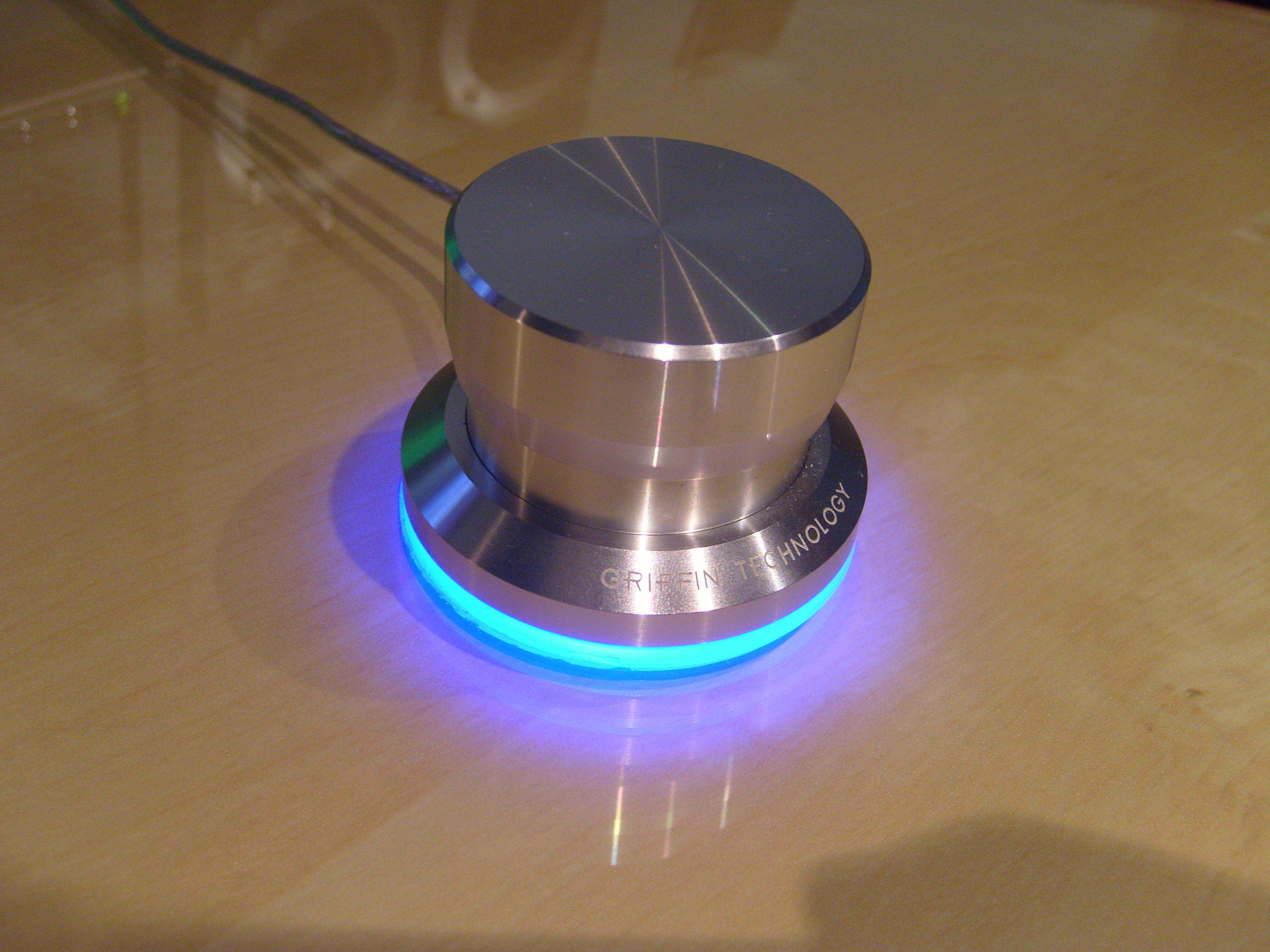
I forgot when I did during all of this, but I did get an Airlift to poke around with the libraries and such; I was kinda curious with the WiFiManager class that should make it easier to stay connected. Another Adafruit library I found was their NTP library, which is super simple to use. The NTP object is created with the Airlift object, and .set_time() is called on it to set the MCU's time (the MCU of the board, not the MCU of the Airlift). .valid_time is provided to be able to know if the NTP sync was successful or not. Setting the RTC to the MCU's time is just as easy, as it just takes rtc.datetime=time.localtime() to do so if the sync was successful (probably obvious, but time.localtime() is the time from the MCU). This was another reason that I decided that this project would be better than the Raspberry Pi clock, as I had a lot more unanswered questions with the Raspbery Pi clock that would require testing I didn't feel like putting in the effort for. One of them was if I was still able to access the RTC if it's given to the system, and I had assumed not, so setting the clock via the OS required a shell script and tweaking the list of sudoers was the route I would've needed to go. The other question was if I would even be able to access the I²C line at all, because of the former. With this project, I have a lot less worries about the I²C lines and device access.

I did also use the ATSAMD51J19A-A dev board to test out the automatic syncing of the RTC module I have, and it worked fine since I had to set the RTC module time for the third time. I forgot which project I was working on, but I was using the RTC module to test out the 32kHz output pin and when hooking it up, I didn't realise that I swapped VCC and ground, so while I got nothing, the RTC, board, and backup battery were heating up. I forgot how I realised it, but I did and unplugged the board while heading to the soldering station for one of the fans to cool it down. I was worried that I fried the RTC, but when it was cool enough, it worked just fine and had just lost the set time. I think I had read in the datasheet or somewhere that the 32kHz output only works when the RTC recieves power on VCC, so it was what I was trying to test for, but I didn't have any luck getting a good reading. I had also read that I would need a pull-up resistor for the 32kHz, and I had soldered a 2.2 kilohm resistor according to the post I read (datasheet says anywhere between 1k and 1M) before the test. I also had desoldered one leg of the resistor during the test because I was having troubles getting a reading, but it didn't seem to make a difference. I was using the oscilloscope I use at work because it was more convenient than the one at home (which is some leftover one from work), but got some funky waveform, and tried it on the the oscilliscope that the electrical engineer uses and still got the same weird waveform. I think this is what sparked me to try the one I have at home and either I had the reversed polarity fiasco then or it was before all this, I really can't remember. Regardless though, I ended up getting the frequency metre to read the 32.768kHz it was supposed to read and the wave was square and was close enough to 32kHz. I took the RTC to work again the next day and also got the correct waveform. I know I had some sort of suspicion that it might have something to do with the ground line of the oscilloscope connected to the bench power supply, but it didn't seem to be it. I think with the initial test with the oscilloscopes at work, I did try using the little probe grounding thing with no avail. Dunno what happened, but well, I got what I was looking for in the end. The second time I did the reverse polarity thing was while setting up for the automatic syncing test, and well, I had more of a reason to do it after it cooled down enough.

Anyway, the reasoning for the 32kHz output pin was to see if I might be able to use that instead of having a dedicated crystal circuit for the MCU, and from the post I previously linked, it should be doable. I checked the datasheet for which pin to connect to since one of the two crystal pins is the output and one is the input. I keep forgetting where I read it (it was some Adafruit thing, I know for sure), but the MCU uses the USB pulses for timekeeping on boards that don't have a crystal (or something like that). Since the clock would be connected to some USB charger, it probably wouldn't get the pulses, so I needed to add a crystal in some way. Using the 32kHz output was a lot more space efficient because it would've been a tight fit to get a crystal and its caps near the crystal pins (PA00, PA01). Routing was kinda interesting because I was thinking to redo some traces and kinda take a long way around, but decided to try running it the other way while hugging other traces, which ended up being easier. I only needed to redo the placement of the 6 ground-stiching vias and the via of the 3.3-volt bus on that side.

I don't know if it's the most dense board that I've designed, but it's definitely one with a lot of minimum-width traces. I think that's really all I can say about it until I get boards and stuff. Silicon shortage is also affecting MCP32017 supply as well as the MCU, so double ouch in this case.

While writing this, I (obviously?) had the board layout open and such and was questioning if the extra voltage regulator would really be enough, since the theoretical maximum current draw of the display at 2 volts (their forward voltage) is 640mA. This made me want to try to measure the actual power consumption that the Airlift is using (at the 3.3 volts), and while it should be manageable by lifting the output leg of the regulator and soldering a wire to it, when I actually looked at the physical board, I didn't feel like taking the time to trying to do so. At that point, the friend that helped me name i3rd asked if it might be in the datasheet, and well I hadn't thought to check. While the datasheet doesn't give any meaningful current consumption, I did find that they recommend a minimum of 500mA supplied to the device, and with Adafruit having the 600mA voltage regulator on the Airlift board, it's probably safe to say that I can expect at most that. I did find some voltage regulators that have a maximum output of 700mA and 1A, and probably will use the 1A version so that I really don't have to worry. I was thinking to not have the Airlift's regulator add to the 3.3-volt bus on the board, but it'd probably be for the better that I don't. I might've been fine with 600mA and whatever is left over from the Airlift's regulator, considering that I don't plan on actual 100% brightness for full brightness, but desoldering the regulator to replace it will be annoying.

28 June 2021

Apple Keyboard II Revival

For those that might remember, I originally tried to revive the Apple Keyboard II with a Teensy 2.0 (link), but it ultimately failed. I did kinda poke around with it again recently, but still couldn't get it to work. Anyway, with my CircuitPython/MCU "craze", I decided the next best way is to just make my own controller board for it.

The first thing to do was to figure out the array of the membrane keyboard, which was annoying to do but still doable. What was interesting to find was that the modifier keys (control, shift, option, command, caps lock) had their own rows but all had ground as the column. Another interesting thing I found was that the right and left shift keys were tied together, so pressing left shift is no different than pressing right shift — they were both on the same row. I used a spreadsheet later on to clean up the array map and to map the positions of the membrane to the MCU pins.

Another thing I had to do was to get some of the board dimensions and such, but it was a little tough to get reference points because the board's size from the tolerance that Apple put in. I figured out to use the centre of the tactile switch as a reference point because there's a boss in the case underneath the board where the centre of the tactile is (or rather, supposed to be because the boss' circle and the tactile switch's circles are not concentric). I had to go back a lot to get dimensions that I didn't think about and it was a bit annoying having to get the keyboard out and open it multiple times.

I was thinking to use the original FPC connector and desoldered it before measuring the via spacing on the board for it, and came up with some weird numbers, but kinda went with it. I had also looked to see if I could find something that was close or would work, and I think I had found a part, but it was obosolete or non-stocked. Later on, I thought to check the entirety of the spacing or to take the spacing and divide it accordingly, and with measuring centre to centre of the first and last vias, I found that the spacing I originally had wouldn't've worked; I think I also confirmed the issue with the spacing on the keyboard's FPC cable. With this, I realised that the connector was metric and searched for a part using metric dimensions (1.25mm pitch instead of 1.27mm) and found a compatible part that's active and in stock. Looking at its datasheet, I decided to go with it because it was narrower or shorter (I don't remember which) than the original part, which would give me a bit more board space.

One of the things I wanted to keep was the ability to plug the keyboard in from either side, but this was a little easier said than done because I wanted to keep the board cost as low as possible and also trying to avoid running long traces for the D+ and D- USB signals. I decided having remote boards would probably be the best option, but I would need to connect them. For the right side, I decided to use an internal USB cable because of the ~20cm distance, and for the left, I decided on an FPC cable. Because of the internal connections, I wanted to have a way to be able to check if the cables were connected (well one of them would have to be connected for the MCU to get power to do so), so instead of having just 4 connections for each USB signal, I needed 5. The FPC was easy, but the internal USB connection gave me trouble. I wanted to use USB-C because of its size and such, but it seems like the spec says to connect shield to ground because of all the USB-C cables that I have, shield is always tied to ground. What I needed was a shield to shield connection so that I can use it to carry the high signal from the MCU over to the remote board where it would connect to ground (getting the far-side connection status is more useful than the near-side connection status). I had also thought about using USB micro-B, but it was hard to tell if the shield-shield connection was there in the datasheet, and there wasn't any connectors that were easy to hand solder fully (there's usually a couple pads underneath the shell that requires solder paste and reflowing to fully secure the connector to the board). I settled on using USB mini-B on both sides and using a short USB mini-B cable (USB A male to mini-B male) and a short USB mini-B adapter cable (USB A female to mini-B male) for the connection between the boards, and confirmed the shield-shield connections in both items. For the USB connection between the keyboard and the computer, I went with USB B because it's the only option to fill out the ADB port (really, a 4-pin mini-DIN) cutout.

With two USB outputs to the computer, I needed to keep them separate for minimal weirdness, so I opted for a signal relay to do this. I connected a diode between the 5 volts of the USB and the 3.3-volt voltage regulator to keep the two 5-volt lines separate, and behind the diode, I have a small trace running to an inverting level shifter so that the MCU would know which side the power's coming from and adjust the latching relay accordingly. The main problems were that I had the FPC connector for the keyboard in the middle of the board, I wanted to keep the USB traces on the board as short as possible, and that the relay and USB mini-B connector take up quite a bit of space. I also wanted the MCU on the top side of the board to kinda show it off (well, whenever the keyboard was opened up), but I eventually opted to put it on the bottom of the board because I didn't have any other choice. I was going to use a latching signal relay that I had used before (probably one of the soundcard switching ones) which takes up a small area while being kinda tall, but I had to switch to one that took up more area for a reduced height. Originally, I wanted the relay in the top-right corner of the board because of the amount of space that's above the board, but to keep the USB traces sane, I moved it to below the keyboard FPC connector. I also wanted the mini-B connector in the top right, but again, sensible trace routing made me move it to below the FPC connector.

Exact placement of the MCU was weird, it had to be above the FPC vias, but had to keep the pads and traces away from the boss under the tactile and the stabilisation boss next to the tactile. I put the pad egdges a millimetre away from the FPC vias, but had to wait until I had the airwires and some traces in before I could figure out its x position. I also had to do some pin swaps and rerun traces to make it a little easier/cleaner and such.

At some point, I decided to add a piezo buzzer for num lock indication originally, but it evolved into also indicating a broken internal connection (assuming the MCU can get power) and indicating that both sides of the board are plugged in (which would probably very difficult to do, but if it did happen, the MCU wouldn't know which way to switch the relay). I think the piezo buzzer was another piece that made laying out parts weird? It went into the top-right corner.

Board retention is another issue, and I decided to have a 3D-printed part that would make it so that I could screw the boards to the part and set the assembly into the bottom case for the boards to be in a stable position and to not have to try to design the boards for friction-fit placement.

The (likely final) mainboard with notes and such.

I wanted to try to make one board for both sides, and there was a lot of back and forth between being able to do so and not, but when I did straighten out the insides of the case, I was able to do one for both sides. I was wanting to use the through-hole USB B connector that I used for the cooling/charging station that I never talked about, but because the nature of through-hole parts and the way the board would be, I decided an SMT version would be better. The problem with the SMT versions is that the pads for the shell were not within the design rule region because of where I had the edge of the board, but eventually I moved the edge of the board a little further away because there wasn't anything else I could do. Placement of the other connectors was weird because I had quite a bit of space for the FPC connector and I didn't have a length for the board yet. I think it was after getting the mounting holes and such that I was able to get the connectors into place. With the FPC connector in place, I was able to get a distance to base the length of the FPC cable on (since pre-made FPC cables come in certain sizes and is cheaper than making my own via OSH Park).

The remote board and such.

The caps lock key is kinda unique in that it is a locking switch, so it clicks into and out of place when you turn it on or off, and because modern keyboard controllers just toggle the caps lock state, this presented a problem. Back when I was fiddling around with the Trinket M0 and keyboard HID library, there was a way to get the lock status with the USB HID library, but it was awkward, but with some update, it was moved to the keyboard HID library and was easier to use. Anyway, the way to solve the problem of properly sending the caps lock toggle with a locking caps lock key is to send the key input whenever the state of the switch is not the same as the caps lock status. For handling the keyboard keys, I used Adafruit's matrix keypad library, which made it a lot easier than having to write the code myself (and I was ready to because I knew how to).

Because Apple's numeric pad section is different than ones for PCs (even still to this day), I was going to move keys around to keep the layout consistent with PCs, but because Apple still uses the same layout, I moved them all back. There is no num lock key, instead it's "clear", but since it's the same key ID, it would be num lock anyway. Because they clear key would be the num lock key, there had to be some sort of indication for num lock status, which I solved with the piezo buzzer. Whenever the num lock turns on, the buzzer sends two ascending notes; the buzzer would send two descending notes when the num lock turns off. I did it this way instead of using LEDs of some sort because I didn't want to modify the case. I also had an idea to use a level shifter to drive the piezo at 5 volts instead of 3.3, and while it is louder, it doesn't seem to fully like it. I also need to test it with a transistor between the piezo and ground to control the volume, so that it might be louder than when at 3.3 volts, but doesn't do the weird thing that it does at 5.

I have the power button set as a funciton key and have a filter set in the code so if there's a set function key, it would strip the corresponding keys out of the pressed keys list before inserting the new key. For example, function and left arrow I have set as home, so in the list of pressed keys, left arrow would be removed and home would be inserted into the list.

Besides the silicon shortage screwing with MCU availability, I still need to get the dimensions I need to CAD the "liner" piece that holds the boards, and I also need to CAD the piece that helps reduce the movement of the USB B connector.

25 June 2021

Extended 10-key Keyboard

I wanted the extended 10-key (or numpad, same thing) keyboard kinda badly with the influx of MCU projects, and because it wouldn't be too worthwhile to try to do it with reed switches like I wanted (considering I still have to design the new mechanism and figure out how to get them made), I went with the good ol' Cherry MX switches. I forgot how I had the layout for the reed switches planned (forgetting that it was in the backlog for this blog), so I went and created a new layout. Seems like the reed switch layout doesn't add too many keys while the new one I made adds much more.

The new layout. More on how I made this image later.

I did get shift and tab where I originally had planned, since the point of having shift on the opposite side of enter is to be able to move upward in a spreadsheet, but couldn't remember anything else, so I thought about the keys that would be most convenient to have. I also wanted the four "extra" keys that my keyboard has because I plan to eventually shift to a 80% (or ten-keyless, TKL) keyboard and don't want to lose those keys. For EAGLE, I usually have my right hand on the trackball and use my left hand for numeric entry when I need it, so the other feature I wanted was to be able to solder a mirrored version from the same board. I also wanted backlighting since I think I already had the NeoPixel Nano 2020 RGB LEDs for the Powermate, and the datasheet gave me the dimensions of the LEDs, which I used to confirm that they would fit in the hole in the bottom part of the Cherry MX RGB switch shell.

The board does extend beyond EAGLE's free user boundary, but because the board files are just fancy XML files, I had quite a few things that I had to place by editing the file that way. Because of the extra space between the Fn4 and Backspace keys due to the Backspace key being two keys wide, I decided to put the USB mini-B jack there, and the MCU (ATSAMD21G18A-A) close to it. The LEDs were placed, but the voltage in (VDD) stayed unconnected to the board because I wasn't sure if I was going to power them with 3.3 or 5 volts, and I was somewhat concerned with the theoretical draw of 1.044A (5 volts) at full brightness white. I went and made a test board for the 29 LEDs and did what I could to make it as small as possible to keep the cost down. Because of the odd number of LEDs (29), I decided concentric circles would be the best pattern to use, and laid some circles and lines down to help me position the LEDs. The outer ring has 16 LEDs, and I had to tinker a bit to get those reference lines drawn.

The equations used, jumper part number as a reminder, and the board.

After getting the board made (with other boards, etc, etc, etc.) and in-hand, I soldered the LEDs on starting from the centre and working my way around the ring before working outwards. For testing, I think I just had the script go to full brightness white immediately, and on 3.3 volts, the 3.3 voltage regulator browned out and reset due to it only being able to provide 600mA. 5 volts was fine, but I was too dazzled with how bright it was to realise that I wasn't supposed to leave it on for very long, and when I touched the board for whatever reason, it was pretty hot. I immediately unplugged it and shook it off a bit to cool it off, and when I went to connect it all again to check the LEDs, two of the LEDs had burnt out (centre and one next to centre). I went to replace them and started with the centre one, and I decided to double-check which of the ones next to the centre one was dead, but it turned out that I didn't need to replace it. I dunno if I really needed to replace the centre one, and I should've checked since it was annoying to get the centre one off (I used a razor to get under the LED along with large blobs of solder, I think). I had originally thought to use the test board as a sort of flashlight (sometime between when the board was designed and before the test) when I was done using it for testing, but easier said than done when I'd have to figure out how to sink or dissipate all that heat.

For the top row of keys, I did my best to measure the distance between the keys on my keyboard and got about 1-1/64 inches (closest value was in inches, I would've used millimetres otherwise), and used that for the top row distance. I was going to need a custom plate done and really didn't want to use Front Panel Designer because I'd have to draw and lay everything out. Some searching brought me to http://builder.swillkb.com/ which was a little confusing to use until clicking the circled question mark icons. The first field is for the layout from http://www.keyboard-layout-editor.com/ which I played around with to get the layout (as seen in the first image of this post). (Later I found out the layout editor doesn't like my "non-standard" spacing value, and just says to select a valid value within a tooltip with the closest two values, but it doesn't seem to care otherwise.) Anyway, I took the layout's raw data back to the custom plate builder thingy and had to poke around with the settings and guide to get the top plate, but the DXF turned out weird when I downloaded it. I was trying to double-check the dimensions in CAD, but it proved to be weird because I didn't understand the kerf setting that was being automatically applied when I hit the "Order from lasergist" button. (I think I did a bit of drawing in Fusion 360 to confirm kerf? I don't remember now, but I did eventually get my head on straight to understand kerf.)

I left it alone since I didn't really want to deal with it, since I think I was having troubles getting holes for mounitng, but I was able to get them a different way when I tried sometime later, though I had to play with the settings to get the holes where they should be. I think I checked with CAD again and called it good enough (I still wasn't getting the kerf thing), and made notes of the settings so that it'd be less stuff to remember when I go to actually order the plates.

Because there's seven keys that are two-wide, I needed stabilisers, but had nothing to go off of. I think it was when I was digging for stabilisers when I came upon a PDF file that Digi-Key happened to have that had quite a bit of info on the Cherry MX switches. I saved this goldmine of a PDF because it provides more info than Cherry does nowadays (I think I ignored the stabiliser part numbers in the PDF because the PDF seemed kinda old and I didn't know how trustworthy those part numbers would be because of it) and there was no telling when it might disappear from Digi-Key's servers. Anyway, I found some stabilisers that seemed to be cheap enough and seemed to be the plate-mounted stabilisers that I needed (there was only two images and it was hard to tell anything because the parts are black plastic), and I ordered twenty-one of the stabilisers. When I got them, it didn't seem right, and when poking around with them, I found out they were PCB-mounted stabilisers. Since the store had a no returns policy (yay small operations specialty stores), I had no choice but to eat the cost. I did end up finding a few places with the plate-mounted stabilisers, but the prices were more than the PCB-mounted ones that I had bought. The store with the best price because of a quantity discount had the highest shipping cost because the store's in Taiwan. Sure, I could make the shipping more reasonable by buying more (or by buying the parts separately in bulk), but I didn't want even more stabilisers sitting around. I held onto the next cheapest place (that sells them singularly and not in sets that include a spacebar stabiliser) as I decide to give the part number from the PDF a shot. And it was a good thing that I did, because I think the search gave me a result from Allied Electronics (which I bought some Cherry MX switches from before for the original spring mod) and I think also Digi-Key. Digi-Key has it as a non-stocked item, so I saved Allied as I went to Mouser to see if they had it, and though they did have it as well, it was non-stocked. What was curious with the result is that there was another result that was the part number without the dash that was in-stock, but because it (as well as the full-hit result) had no images, it was hard to say if it was the stabilisers or not, especially when it's listed as "Switch Hardware 1x2 KEYCAP W/FRAME" with "CHERRY" as the manufactuer (the full-hit result is listed correctly).

When I was ordering stuff from Mouser (I think the stuff for the other MCU projects that was in-process), I went ahead and ordered twenty-one of the item that should be the stabilisers, and since it was 0.18 USD each, it was a cost easier to eat if it wasn't (Allied's price for them was probably about 0.26 USD each, so Mouser would be cheaper if it was right). When I got the parts, I think I went straight for the item, and gloriously, it was the plate-mounted stabilisers that I was looking for. With the confirmation of the correct stabilisers, I ordered the top and bottom plates from Lasergist through the custom plate builder site. (Link to the plate-mounted stabilisers at Mouser for those that want it.)

While I did get an order confirmation from Lasergist, I never got a email that it was shipped, so it ended up just appearing with the post. I had ordered 3 copies of the top plate (that holds the keys and stabilisers) and the bottom plate (which acts as the base) in the shiny 304 stainless steel option (I could only select shiny or brushed stainless steel), and the plates were heavier than I expected (to be fair, the bottom plate is literally just a sheet of steel with four holes and rounded corners).

Lasergist inner packaging (and part of my keyboard).

Is this how you use iFixit's metal spudger?

The plates freed from the packaging, and the front and back of the top plate to show the burrs from the laser cutting.

I was going to sand blast the plates myself, so there wasn't a point to selecting the finish when ordering. Though now that I think about it, I was thinking about using Lasergist's ordering system instead to be able to have both sides brushed, but it ended up costing more than if I ordered through the custom plate builder site. I forgot about laser cutting leaving burrs (though lasergist did clean up the top side and polish it), so I had to buff those out, and because I had never worked with 304 stainless steel, I had no idea what to expect. It wasn't as bad as I thought it might be (I just started with one top plate to see how it would go), and I went to grab two bottom plate and another top plate to do. Sandblasting is where it really showed how the metal is, where it seemed to be slightly harder than aluminium but softer than the steel I've sandblasted at work.

Bottom of the top plate after buffing, top plate after sandblasting, bottom of the bottom plate after buffing (scratches were pre-existing), and bottom plate after sandblasting.

Why two? Because I was waiting on a friend (different friend than the Powermate one) to say whether they wanted to keep the shiny finish or if they wanted it sandblasted. Eventually, I kinda made the decision for them and sandblasted them anyway.

Post-sandblasting of the bottom plate. I wore gloves to not put finger oils on it since it's not mine.

Back when I got the plates, I realised that I made a mistake in the PCB design because I had arranged all the switches to have the LED above (y-axis) the switch, so for the keys that are 1×2, there was nothing there to hold the switch to the plate. While it technically is fine to have the switch legs to hold the switch to the PCB, I preferred if the plate holds the switch instead, so I had to turn them whichever way would keep the increase in board size to a minimum (90° clockwise). I also realised that the stabilisers pretty much meet with the PCB (even for being plate-mounted), so I had to draw a mockup footprint to know what I would need to move. After the info from test with the LEDs, I was able to connect the LEDs' VCC to 5 volts in the airwire and be able to run the rest of the traces. Oh right, I also used some polygon pours to connect the 5-volt from either of the USB mini-B jacks, and I had adjusted the design rule to tent minimally-sized vias. There's also a spot for a probe pin that would contact the bottom of the top plate, and a 1MΩ resistor between that and ground to help with ESD (maybe overkill, I dunno). I also did some ground-plane via stitching to help make a direct path from the switches or LEDs to the ground pad of the USB jack.

This screenshot is as good as it gets, sorry.

For the keycaps, I was thinking of buying a set of keycaps for a full keyboard and using some of the keys to fill out the standard numeric pad while using some letter keys for home and end (I had spent time figuring out what to use, and came up with either I, O, or P for home and L for end), and then getting some coloured blank keycaps from WASD Keyboards to fill in the rest. The main problem with this is that I end up with a bunch of unused keycaps at the benefit of having the standard numeric pad labelled, and though the blank keycaps are a little pricey, it is still a cheaper idea. At some point I found that WASD Keyboards sells a kit of their blank keycap colours, so I went ahead and ordered one because it was cheap and I didn't know how much to believe the images on their site. There was some differences (which I reported to my friend that just wanted all-blank keycaps to make it cheaper), but with the keycaps in hand, it was a little easier to imagine. I used the layout editor to kinda build a colour layout, and I forgot how I decided to try the keyboard customiser on WASD keyboards, but I was able to get their colour lineup from it, which seems to have changed a bit since the layout editor was created. (Along with the colours, some of the colour names on the layout editor are wrong, which I also reported to the friend.) Anyway, I wanted to have the 10-key area all one colour so it stood out, and then have all the added keys different colours.

The layout I decided on (unless I change it).

Oh right, the control and shift keys give some additional layers to the four function keys. I haven't been able to do much else (I don't want to order the keycaps yet, since shipping would be cheaper if I ordered mine and my friend's keycaps together) since the bloody silicon shortage, so the project's at a standstill until I get the three ATSAMD21G18A-A that I would need. I'm also wanting to look the board over again before I send it to OSH Park because I don't want expensive mistakes; yes, I could order from somewhere else, but my friend likes purple colours and OSH Park seems to have the best rating for quality compared to other PCB manufacturers that Manufacturing Reports has reviewed (this is the place where I found the "mouse bites" comment for OSH Park boards). I could get the bootloader and CircuitPython built for the board, but there's really no point until I have the boards ordered at the very least. There's probably some stuff I forgot to talk about, but I've been typing for too long.

24 June 2021

ATSAMD21G18A and ATSAMD51J19A Development Boards

For being able to test the custom controller without having to spend money on the board (especially when I wasn't sure if I'd be buying the board without the joysticks or buying the one with joysticks that hadn't been designed yet), I needed at least a development board with the same MCU that the controller would use (ATSAMD21G18A-A). Between Adafruit and SparkFun, I couldn't seem to find a board that gave me access to all of the pins, since Adafruit's usually has a NeoPixel or DotStar along with a discrete LED taking up pins, and I don't remember what SparkFun's was like besides being much larger and pricier than I wanted. The solution was to make my own that has all the pins broken out, is as compact as I can get it while keeping compatibility with 2.54mm pitch headers, and has no extra frills (SparkFun's has one or two extra power inputs).

First thing I had to figure out was what size headers I needed and how to arrange them to keep it as compact as possible without having multiple rows of pins so that it's easy to label. I tried a few sizes and plugged them into my EAGLE helper programme to estimate the cost and took the best one, which was 16 pins by 9 pins for the 21G. By this time I had a standard of keeping the MCU on the same side of the board as the USB mini-B jack so that the D+ and D- lines are easy to connect, which I continued to follow as I placed the jack on the left of the board and placed the MCU roughly in the middle (probably towards the right more). Airwiring the pins to the vias for the headers ended up pretty easy, as the left bottom vias connected to the pins next to the USB pins and I worked my way anticlockwise with both the pins and the vias. For the traces, I started with the bottom pins/vias because it was hard to tell if there was enough space to fit all the traces there, and there was enough space for all of them with the MCU centred vertically. I had to shift the MCU leftward to tighten some of the traces up more, so I kinda had to redo those bottom traces, but I think it ended up looking nicer. The reset button was pretty easy to place with plenty of space on the bottom, as well as the components on top, but the capacitor for the MCU's core voltage (VDDCORE) gave me a bit of trouble for placement because I needed to avoid the silkscreen but keep it as close as possible. I feel like I might've redone part of the 3.3-volt rail to make it easier to place the VDDCORE capacitor? Anyway, I added an LED on the 3.3-volt rail to indicate if there is power or not (another one on the 5-volt rail from the USB would make it easier to diagnose if the voltage regular is working or not, but I didn't think of it then). Running SWCLK and SWDIO to the programming pads was somewhat tricky, and I had to use a slightly smaller trace size, but that's really all that was needed to make the traces as short as possible. Because of one of the vias possibly interfering with the silkscreen dot for MCU positioning, I had to place another one just in case (I think it kinda was okay?).

Very Teensy-looking.

The headers are split up as such because I was only going to buy a couple sizes and break them down accordingly to fit because the 16-position headers were either unavailable or non-stocked. Anyway, the board for the 51J didn't go nearly as easily because of the increase in amount of pins, and I spent quite a bit more time with different layouts compared to the 21G. I think the most ideal board size would leave 3 vias unplaced, and I was also considering having one via come in towards the centre on the bottom and top at the left side, but that would've still left one via still needing placement. I eventually went with a 13 by 12 layout because it was the best that I could do while keeping the board cost as low as possible. I went with the same idea of starting with the pins next to USB and working anticlockwise for doing the airwiring, and also started with the bottom traces first. Even though there were a couple more parts to this one, there was much more space for placement, though I think I redid a couple traces to make it easier to do the reset button. Since I was copying part of the schematic from Adafruit's boards, I only have one capacitor for 5 volts on this one instead of two. Really not a whole lot to say, since there's really not much different than the other one.

See? Not too much different.

The 21G dev board would cost me about 7.19 USD (per three), the 51J dev board would cost me about 12.60 USD (per three), and with both of them totalling 20.79 USD, it makes it cheaper than the 23.50 USD that the custom controller board would cost. Not only is there a savings of 2.71 USD, it saves me from having more boards in my "graveyard" of boards, since the dev boards are much more reusable.

The boards were ordered with a bunch of other boards and their parts were ordered with a bunch of parts for other boards (I feel like I've said this before...), and when going through the parts, I found that Mouser put the ATSAMD21G18A-A MCUs in a regular static dissipative bag instead of the moisture barrier variant, but the ATSAMD21E18A-A and the ATSAMD51J19A-A were packaged correctly (the MCUs have a moisture sensitivity of level 3, or 168 hours). I can't remember if I had the boards first or the parts first, but regardless, I soldered the 21G MCUs to the board as soon as I could, and I haven't seen any weirdness so far. "What's the big deal with MSL?" you might ask? Well, moisture isn't great for certain semiconductors (ICs or not), and for stuff like MCUs, it can make operation wonky. For example: at work, one of the MCUs I work with isn't being stored in accordance to MSL specifications, and when I recently used 14 of them, I had to replace 2 of them because they were the source of a secondary output signal not operating. So yes, the MCU ran the firmware fine, but moisture damaged the operation of a pin. Ideally, the MCU should've been baked in accordance to MSL specifications before use, but I don't have that sort of capability at work, and there's no guarantee that just putting it in the reflow oven for a reflow cycle will dry it out properly. Though I say this, LEDs can be moisture sensitive too (as I mentioned a bit here), but for basic LEDs, it's probably not nearly as important to follow, unless you want reliability across 100% of the LEDs being mounted.

Anyway... The plan I had was to only populate one of the three boards with headers because three of the same board is a lot and the testing for the custom controller required me to make a lot of ground connections, which would be easier to do with the board having vias and not headers. Also the power LED turned out a lot brighter than I thought it would be, but all I would have to do is change out the resistor for a higher value (whenever I do it). Both MCUs were easier to solder under magnification instead of by eye, but that's maybe obvious? It was sometime after this batch of boards that I learned how to tent vias, and I would've done so with these dev boards had I known. Que sera sera.

51J boards, use your imagination for the 21G boards.

I haven't used the dev boards nearly as much as the Trinket M0 or the ItsyBitsy M4 that I have (I purchased the ItsyBitsy M4 with the one shrouded header I needed so that shipping would be more reasonable... I wouldn't have it if I properly counted how many of those headers I needed before making the order), but they're there when I need them. I also made some adapter boards for the flash chip that would socket into the boards with headers to expand the flash space, but I haven't had the boards made because I haven't needed extra flash space. I'd also have to build CircuitPython with the flash chip included in the config, but that's pretty easy (I'd just have to remember to have the adapter board connected before changing variants). I did think of using either dev board to try 8-bit character LCD communication (since I'd have more than enough pins to be able to), but I probably would have to write my own library for that, since Adafruit's library is 4-bit only. Reasoning for trying it is because it should be twice as fast to update the LCD, so on a 20×4 LCD, it should post the entire screen "instantly" compared to 4-bit, which has a slight lag with the fourth line.

23 June 2021

Griffin Powermate Hack

Griffin Powermate. (Image from Deskthority Wiki.)

A friend and I both have a Griffin Powermate that we bought around 2008, which we used for various things, and while it was great in Windows XP, it was pretty much non-functional in Windows 7. There were forums and such saying to use the Vista drivers and running the software in compatibility mode, but neither my friend nor I could get it to reliably work, and so we both stowed it away (or at least my friend did).

I think it was while I was poking around Adafruit or something when I encountered the rotaryio library or the rotary encoder guide, but regardless, it got me thinking about the Powermate. It's a bit hard to remember this initial stuff, since I was also kinda deep diving with MCUs and CircuitPython, as well as working on the 3DS input redirect controller and some other MCU projects.

Anyway, the first thing was trying to figure out how to get the thing apart without doing too much damage or creating more work later, and I asked my friend if they still had theirs, to which they replied that they did. I wanted an extra as sort of a "sacrificial lamb" in case worst comes to worst, though I did also have a link saved to an ebay listing for buying one. One of the images on the ebay listing shows the top cap popped off, and when I was able to try it out on mine, I was stupified on how easy the cap was to take off, but to be fair, I never had a reason to pull the cap off or even try it (and neither did my friend). Below the cap on the main body is a little felt piece that I kinda ignored because I saw a nut that was holding the rotary encoder to the main body, but unfastening the nut didn't yield any meaningful results. Because there is a sort of gap between the bottom and top pieces (you can see this in the above image, especially at full-size), it was more likely that the body is made from two pieces of machined aluminium that were assembled in some way (either by press-fit or some sort of threading).

When I got my friend's Powermate, I first tried to twist the two parts apart, but I couldn't find channel-lock pliers that were large enough for the base (nor did I want to buy one large enough for doing so), and I wanted to avoid the pipe wrenches at work because of the lack of curve in their jaws. I also tried a trigger clamp, but it ended up slipping from the lack of surface area. Looking at the bottom at the glue that attaches the plastic to the metal, I found a somewhat large spot that the glue didn't spread to (the glue is white btw), so I decided to use the Jimmy pry tool (iFixit) to see if I could pop the bottom off, and well, it was quite easy. I unfastened the nut and went to to desolder the USB wires from the board, which gave me a better look inside, and I saw a more obvious seam between the parts on the inside. I think I tried the pointy side of the metal spudger (again, iFixit) between the moulded strain relief for the USB cable and the bottom part of the body, and it did slowly give, but because of the strain relief compressing, it made it tough to free the bottom piece. I think if I had two metal spudgers, it would make it easier to separate the parts, but I still got it apart with just one. I felt a little stupid for not trying that before popping the plastic piece off of the metal, but it wouldn't be too hard to glue it back on.

With the new separation strategy, I applied it on mine to be able to get the board from mine, and because I was already at the soldering station, I went and desoldered the rotary encoder from the board, which was easier said than done with a small cone tip (I should've used the larger cone tip for more thermal mass). With the board and rotary encoder, I went to pull measurements for the footprint I would need, and it was a little tough since I damaged some of the vias and ripped off one of the retention pads. Measuring the vias was a little tough, even with pin gauges, but I think I ended up with something that worked, and even getting the placement of the rotary encoder footprint position on the board was also a bit tough since the board has what someone calls "mouse bites" at the north, south, east, and west locations (which can be seen in the larger versions of the board images below).

Bottom of the board, top of the board, body bottom (with marring from the metal spudger).

The board was fairly easy to design, since I was using an ATSAMD21E18A-A, which fit in between the button and encoder legs of the rotary encoder, and I had to put a reminder in my notes that I would need special pads for connecting the programmer to the board and that I would need to figure something out for the reset button. For the lighting, I went with sixteen RGB LEDs (specifically, WS2812B-2020 aka NeoPixel Nano 2020 from Adafruit), and this was because it seemed to be a good density, along with the fact that I already had the placement equations from a test board for another project (extended 10-key, more on it in another post). (I think I already said it last post, but I was working on a lot of these CircuitPython/MCU project in a short amount of time and/or concurrently.) Anyway, I had a realisation moment that I could also do twelve LEDs instead and made a copy of the board to reduce the LED count and reposition them accordingly. I think part of this is because of the theoretical current draw, which is theoretically 12mA per colour (according to the datasheet), and translates to 36mA per LED at full-brightness white. With 16 LEDs, the theoretical current draw is 576mA, and 12 LEDs drops it to 432mA. I was trying to keep the current draw under 500mA, which is the USB 2.0 spec, so I decided I'd order both versions of the board and do some testing to see if there was going to be a problem, since I have a charger that outputs 5 volts at 500mA.

The board designs for sixteen and twelve LEDs.

I ordered the board and parts for the board with other boards and parts for those other boards, and when I had everything, I soldered the LEDs first because of their moisture senitivity level of 5A (I have 24 hours to mount the device or place them into correct storage after opening the bag). Though I did solder one just fine by eye, it was a lot easier and a bit cleaner with magnification. Also, I did use the bench grinder at work to get rid of the breakpoints on the board (aka "mouse bites"). For the test, I would be using the Tinket M0 and just connecting one of the MCU pins to the level shifter on the board, so the level shifter was the only other thing I soldered to the board (I might've soldered the cap for the 5 volt near the 3.3-volt regulator, but I don't remember. Anyway, I had a programme on the Trinket M0 to set the LEDs blue at 5% brightness to indicate the start of the test, and then it would set the LEDs white at full brightness for 5 seconds before setting the LEDs green at 5% brightness to indicate the end of the test. Honestly, I didn't realise how bright the LEDs were going to be and either were practically a flashlight, I felt like I created a monster (XD). Anyway, the charger seemed to keep up with the 16 LEDs, and I might've modded the code to just have it stay white at full brightness, but I don't remember. There's the possibility that the charger might have an output higher than 500mA, but it was the easiest way to test that I thought of that didn't require making some sort of jig for the bench power supply that I have.

The next thing was to create some animations and such for testing because I wasn't sure if my friend would want 12 or 16 LEDs, and I still had the test wires soldered to the boards, so I'd be able to just run the wires out of the USB hole in the body while having the body pieces stacked so it would be assembled enough to not let light leak. I ended up using the loose rotary encoder (I hadn't desoldered the rotary encoder from my friend's board yet) to help keep the board in position with the loose assembly, and it was kinda hard for me to tell the difference between the 12 and 16 LED versions, even with the "chase" animation that looked pretty bad because of the light bleedign to the opposite side. I kinda wished I had another dev board to be able to test side by side, but I made do with what I had. Kinda poking around, I was wanting to see the brightness difference between the single LED on the original board and the 16 LEDs on my board, and though the original LED wouldn't come back on after resoldering the USB, I found that the LED was powered by 5 volts with a bit of probing. I tried to take a picture, but it kinda tones down how crazy difference in brightness.

Left is old LED, right is new LEDs. Seriously, I really did feel like I created a monster.
You can tell with the cap on the left one that these are loosely put together.

It kinda took a while before I was able to head over to my friend's place, but I did show it off to get a decision, which ended up being the one with 12 LEDs for less brightness (even though the brightness is controllable, but whatever). With what was goign to be used decided (I ended up taking the 16-LED board), I desoldered the wires from the board and soldered everything else on (even the capacitors on the opposite side of the board from the USB holes, even though it was proven to be fine without them).

The boards mostly ready for programming.

For the bottom pieces of the body for my friend's Powermate, I found the white glue stuff scraped off pretty easily, so it wasn't too bad to remove, and I was at first thinking of using superglue, but then I remembered I had some clear jeweller's glue stuff (B-7000, but mine might be a knockoff?) that might be a little better because it's not super thin. Before I put the glue on, I went and got a couple trigger clamps to be ready to clamp the pieces after gluing as well as keep them clamped together as it cures for 48 hours. I had to remove the excess glue after curing from the inside and outside, and the latter was easier to do than the former. Because of the clamping and such, there's 100% coverage of glue between the plastic and the metal, unlike whatever Griffin used, and it's also clear (which doesn't make any difference).

I think I was waiting on building the bootloader and CircuitPython because I would need to clone Adafruit's Git repositories to be able to do so and based on some experience with Git repositories, it can take a while if there's a large history/archive or whatnot. After finally taking the time to try it, it didn't seem to take too long until git submodule sync or git submodule update (I don't remember which), but after it finished, I was able to make the necessary folders (one in the bootloader repo and one in the CircuitPython repo) and get all the copied config files changed accordingly. Building was easy and quick (I probably didn't need to add -j32 to the build command, but I did anyway), and CircuitPython and the bootloader were ready. Soldering the USB cable on and soldering the programming wires to the pads were the only thing left for the board to be ready for the programmer, and I followed the CLI instructions because it should work and I wanted to avoid having to use Windows in some way (Adafruit's guide on programming the bootloader uses Windows). Anyway, it worked just fine and the "boot" drive showed up after the MCU rebooted, which meant that it should be working fine and I could install CircuitPython by dropping the firmware file onto the "boot" drive. After the MCU rebooted again, the CIRCUITPY drive showed up instead, which meant that CircuitPython is running, and poking into the serial console allowed me to just run some test commands. I think I was a little weirded out when I saw that CircuitPython was an alpha of version 7, but I thought it should be fine, since everything should run fine. Nope. It gave me a version error for the libraries, and trying the correct version of the libraries still gave me the same error. I went back to the CircuitPython building guide and read over the part that I skipped over, which told me how to switch the version of CircuitPython before building (remember, RTFM means to read everything and not just the parts you think are applicable), and after building CircuitPython 6.2.0, I went to install it on the MCU (the board is still hangin' out) after getting back to the "boot" drive (double-clicking the reset button). With the stable version of CircuitPython running, I was able to confirm operation (I think I was still using the LED test script that had the animations), and the board was ready for the rotary encoder and final assembly.

Friend's board ready for final assembly. (Something that was stored with their Powermate screwed with the clear cable, so disregard the yellowed/blackened spots.)

I think I was going to use the trigger clamps again to press the two body pieces together, but I ended up not needing to do that because I was able to do it entirely by hand? Which would make sense, since it's cheaper to make it so that humans can press the pieces together for less labour/tool costs. Regardless, I don't remember that well. Anyway, the renewed Powermate was ready for getting the final script together and tested.

Friend's Powermate after assembly.

Because the Powermate supported five input types (pressing the button, clockwise turn, anticlockwise turn, holding the button while turning clockwise, and holding the button while turning anticlockwise), I wanted to keep that same funcitonality intact and had an idea of how to do it, but was waiting to be able to test it because I didn't want to use the same awkward setup I used for tinkering with rotaryio and the rotary encoder. The idea I had did work, it's just that the timing needed a bit of tweaking. Originally, the Powermate had a companion software to translate the inputs into actions based on the active programme, but I believe that was part of its downfall past Windows XP (Vista doesn't count because hardly anyone used it). Anyway, replicating the software is easier said than done, and was not something I was wanting to do. I wanted to keep it literally plug and play: no software to configure, no drivers to install, etc. To have separate "profiles" within the Powermate, I created a framework that would have seven profiles (could be expandable if desired), and each would have their own colour (yay RGB). I used the "holding the button down while turning" for changing profiles, so when holding the button down, the current profile colour would come up and turning clockwise or anticlockwise would change the colour and the profile. Though this reduces the functions from 5 to 3, with the profiles, it expands it to n×3 (where n is the number of profiles), and so 21 functions total in the case of the framework.

Profile changing demo. Colours are really washed, but the order is red, orange, yellow, green, cyan, blue, magenta.

Unfortunately my friend wasn't very responsive of what they wanted their Powermate to do, and I just threw the suggestions I gave into the code and called it a day. Was a little annoying that I made the framework for nothing, but oh well. For mine, I have the button trigger play/pause because the only dedicated media buttons I have for Pod is the ones on the speaker remote, which doesn't work if the speaker went to sleep; turning just turns the LED on or off (in a sort of pinkish colour); and I just left the framework for hold and turn because I really didn't know what else to do with it. I could've used it as a volume adjustment, but whenever I actually adjust the volume, it's usually only by one step of 5% and the adjustment is tied to the speakers because I have the speakers connected via USB (the speakers don't seem to like anything less than 3% volume increments).

I recently found a debouncing library, and might play with it for the button, but because my friend's button only turns the LED on and off, I'm not worried about it. Also CircuitPython 7 will introduce ways to hide the CIRCUITPY drive and such, but well, it's easier said than done to get the "boot" drive to show up since there's no way to press the reset button without disassembling the Powermate. I kinda wanted to sandblast the Powermate to get rid of Griffin's markings, but I ended up leaving it alone because I wasn't really wanting to separate the metal from the plastic, mask the plastic off, or sandblast the plastic with the metal. I was kinda awestruck for a while when I got it working (probably after loading CircuitPython 6.2.0) since it was a bit hard to believe that I got my first finished MCU project up and running with no problems. Though I'm not fully utilising it, it still was a worthwhile project to turn something hardly usable into something usable.

22 June 2021

3DS Input Redirect Controller

With some mention of a Discord server member having a modded 3DS firmware, I kinda decided to look into it, and after reading the instructions, it seemed pretty easy to do. I grabbed my secondary 3DS (because I pretty much had nothign to lose on it) and gave it a shot; it really was that easy and non-destructive.

One of the features is being able to control the 3DS with a controller connect to a computer over the network (obviously using a programme on the computer as well), which is pretty nice since the 3DS' directional pad is a little annoying for me to use (I guess I have larger than average hands?). For controllers I have the XBox 360 controller, the Horipad, the Joy Cons, or any of the Bluetooth SNES controllers (8Bitdo or Nintendo) to choose from. The Bluetooth SNES controllers are automatically out for not having a joystick (though probably not a huge deal), the Joy Cons I don't want to have to bother pairing/repairing, the Horipad is wired and connected to the switch dock that I don't want to have to bother with, and so that leaves me with the XBox 360 controller that gives me some disassociative issues because its buttons feel much different than the 3DS'.

With learning CircuitPython, I decided to make my own controller that has a few buttons to allow me to run a predefind macro that speeds up what I was doing a lot by hand; it would also have tactile buttons that'd probably feel a little closer to the 3DS than the XBox 360 controller does.

I think while using the Trinket M0 to do some tests, the programme to send the input to the 3DS didn't seem to register any of the buttons in the gamepad library for the directional pad, and while it sucked, I figured out to just emulate the directional pad by sending a couple joystick movements to make it seem like the joystick was flicked in that direction.

I think the code came first because it was easier to handle? On top of working on this project, I was also learning things about microcontrollers along with CircuitPython. It seems like I was originally planning on using the ATSAMD21E18A-A because it would fit all the inputs as well as having an analogue selector switch (using some resistors and a switch) and four function/macro buttons. Or at least so I thought, because at some point, I realised it took away PA24 and PA25, which were needed for the USB connection to the computer, so I decided to stick the axes of the two joysticks on an I²C ADC (ADS1015) to free up PA24 and PA25. I also had realised at some point that I could use an RTC for the year, month, and day for part of the macro instead of having to manually input it myself, and so I added added it to the I²C line.

I think I started writing the code at this point? (Seriously, there was so much going on that it's hard to remember everything in chronological order.) And with how long the code got, I was uneasy with how large the code was getting and I didn't know how much of the MCU's flash space would be left after all the libraries I needed, so I decided to add an SPI flash chip for expanded storage (it was at this point I hadn't had the Trinket M0 yet). Because of this, I needed four more pins from the MCU that I didn't have, so I opted to "upgrade" to the ATSAMD21G18A-A for more pins. It was likely around this time that I had to look for some other I²C pins because the SPI flash is normally connected to PA08, PA09, PA13, and PA14, and I had PA08 and PA09 planned for the I²C connections. I ended up using PA22 and PA23 for I²C, and then had a couple pins leftover with all the other inputs connected to their own pin. I think I was also just going to use a CircuitPython build for a board that was similar, but after a bit of digging, I became less sure that was a good idea.

I forgot how I ended up with needing a second selection switch, but it seems like I ditched the joystick axes to be able to fit them in? Anyway, I designed the first version of the board after getting some data (button spacing from the Joy Cons), and I think the board sat without traces and airwires for a while before I bucked down and started to do it. I had a bit of problems with placement of the flash and RTC, as well as running the traces for them, but did eventually figure it out. The I²C lines for the RTC was the most annoying because not only did I need to connect the two pins to the MCU, I needed to connect them to separate pull-up resistors as well, but the other problem was getting the trace for the backup battery to the corresponding RTC pin while keeping the trace short and reasonable, and a friend suggested to run the trace in the space between the pull-up resistor pads, which I failed to see (I was getting tired).

Section of the board with the flash, RTC, MCU, part of the backup battery holder (CR2032), and some of the buttons.
If you see the problem with the I²C lines, I'll get to that later.

I think it was sometime after this when I had the Trinket M0, and loading the necessary libraries onto the MCU's flash (the Trinket M0 doesn't have an external flash chip) showed me how much space I had left, which is more than I originally thought. I think I had to strip all the comments and extra whitespace out to really be sure it'd fit? Anyway, since I confirmed that I'd have plenty of space, I could remove the flash chip and shift the pins around a little to have enough analogue pins free for the joystick axes again (even if there's no board space for them).

Sometime I found a guide on building CircuitPython, which includes a link to a guide on adding a new board to CircuitPython, and the latter guide lead me to the configuration files that I'd need to change. Or maybe I came upon it some other way? Regardless, there was the pins.c file with the pin names that board uses to make it easier for the programmer to reference in code, and while I really didn't want to have to make names for it, I did anyway. Later on, I discovered microcontroller.pin that invalidated the need for this.

I forgot to mention, but I think it was around the second board revision (I at least had the Trinket M0) that I found a different version of the input redirect programme for the computer that allowed button assignment, so I was able to give the programme specific buttons for directional pad and allowed me to get rid of the virtual joystick flicking thingy I was doing. I suppose I'll talk about the programme more here. Anyway, the programme (either version) has a window that the user can click on to send the coordinate touched to the 3DS (emulating the 3DS' touchscreen being pressed at that point), but the problem with it was that it wasn't very accurate. The programme allows a specific point to be sent (using L3 or R3 as the trigger) and the point that I sent didn't correspond with what the 3DS says it received (if I sent 205,198, it'd say 208,201). What I tried to do at first for compensation (because I needed the macro to move the mouse and click on the touchscreen emulator) was to get screenshots and scale them down and figure out the translation of points, which kinda worked... Eventually, I found points that corresponded and found that the weird scaling issue is from the horizontal center and below vertical center of the screen. I think at this point I tried poking with the source code (I had to compile the programme anyway) to try to get it to work correctly, but no luck.

I had decided to gather a bunch of points and try to figure out an equation to fix the problem, but I couldn't get anything to work. I think I tried to get an equation from a scatter plot, but I think it kinda worked, but I think I figured it'd be more accurate if I got more points. I then collected literally all the points on the x and y axes to plug into the scatter plot (just one axis though, considering that the scaling is different for both axes), and while it took a bit to get them in, I had something much more accurate (I think I had played around with the dead zones a bit, but don't remember if the final equations included them or not) to work with. After modifying and compiling the code (for the umpteenth time), the coordinates were spot on, except every so often where a pixel would be skipped (it would go from 25 to 27, for example, but be fine after that until the next one), which was good enough because it was much more accurate than it was with the original equation. Because the programme (the one with the button assignment) also allowed the touch emulation window to be resized, it also included some maths to compensate for that, so I had to tinker around with it. I couldn't really get it to work with the window resize, so I ended up just locking the window at a fixed size instead to avoid the hassle.

While the untouched equation for the touchscreen emulation is fine by logic/mathematics, for some reason it just didn't work correctly in Linux, and I kinda did want to try the Windows version (which I think there was a pre-compiled package for), I didn't want to have to reboot to Windows or use Bazett. I might've done a quick test in windows, but I don't remember. I also had tried tinkering with the sent bits before tinkering with the equation and stuff, but that just made the emulation not work most of the time.

It was towards the start of the project that I was planning to have one set of buttons and joysticks and have two microcontrollers so that I could connect to two computers to control two 3DS units with one controller (yeah, it'll do the same thign on both units, but it makes stuff like pokémon trades easier), but after trying to just run the input redirection programme again and just changing the IP address in the second instance (I had applied the mod to my main 3DS at this point), I didn't need to do that. This idea is why I had gotten an ADS1015 breakout from Adafruit, because the Raspberry Pi doesn't have analogue inputs and was also supposed to be the testbed for it. I still did the test, but with connecting the ADS1015 to the Trinket M0 instead, but what I was trying to figure out was if I would be able to connect one joystick axis to two different analogue inputs and get the same values, and it turned out as I expected. (I also had gotten a joystick breakout from Adafruit along with the ADS1015.)

Anyway, another thing I was worried about was how much memory I'd end up needing to run the code and such, but because the Trinket M0 doesn't have enough pins and only has a few pins broken out, I wasn't able to do any testing until I finished my ATSAMD21G18A-A and ATSAMD51J19A-A dev boards. Turns out that there is enough memory to run it if I don't import analogio and add the analogue pins to the programme, but because I had been planning on making another controller that had joysticks, I wanted to keep the MCU the same to make it easier. Obviously the code with the joysticks and stuff ran just fine on the ATSAMD51J19A-A since that MCU has about 6 times the memory than the other, and I went to make another revision to the board using that MCU instead.

Somewhere during this deep dive on these MCUs and CircuitPython (likely between the second and third revisions of the board for this project), I ended up reading about pin muxing (I think for a different concurent project), which I think lead me to save a copy of the IO table from the two MCUs' datasheets before making a spreadsheet with them so that I could sort it by pin or whatever. Before this, I had been relying on the schematics that Adafruit has for their dev boards, but in some cases, it wasn't specific enough. Anyway, I found that for I²C, it was specific pads on the ports that determined which one was SDA and SCL, so while PA22 and PA23 are both I²C pins (on SERCOM 3 or 5), they have to be used specifically. Further in the datasheet gives the specifications that pad 0 is SDA and pad 1 is SCL (there's designations for pad 2 and pad 3, but we're ignoring them for simplicity), and because PA22 is pad 0 and PA23 is pad 1 (again either on SERCOM 3 or 5), PA22 has to be SDA and PA23 has to be SCL. Because I was using the schematic for some Adafruit dev board, it just had PA22 and PA23 labelled as "I²C" without saying which were SDA and SCL, so I had just guessed that it didn't matter or whatever. Turns out that I had the signals swapped in the first and second revisions of the board, but I only ripped the SDA and SCL traces up (and did a pin swap) in the second revsion because that was the more concerning one, even if it wasn't going to be made. I'll be talking more about the pin muxing stuff in a different post for the project that it belongs to.

In my notes, I had the ATSAMD51G and ATSAMD51J as the replacements for the ATSAMD21G if there wasnt' enough memory, but I later found that I wouldn't be able to use the 51G because it's not available in the same package as the 21G along with the fact that it loses one IO pin for a pin that connects to an inductor and such to vary the power input it needs for power savings (if running off of a battery, for example). My only option became the 51J, which was a little larger in size than the 21G, but not much larger (I think the moulded plastic is about 14×14mm compared to 10×10mm?). I wanted to try to keep the routed traces as much as I could, so that I would have a little easier time re-routing, and it made it a bit of a mess while I had to avoid running the design rule check (which would bring up obvious errors). Some inputs did have to shift pins a bit, but otherwise the traces are fairly similar to the second reviison. I also added the connectors for the (Joy Con) joysticks as a placeholder, so that I would be sure I had a path for all the traces (mainly for the left joystick), including the joystick button.

The reasoning for using the Joy Con joysticks for the controller is because of its ease to replace compared to the usual soldered-on variant, and its compact Z-height. While waiting to be able to test the memory consumption of the code, I dug up what I could on the connectors and the joystick measurements, and ended up buying a set of 3rd-party replacement joysticks to be able to measure and confirm the measurements that I found. I had also used it to somewhat mock up an ideal location for the joystick in relation to the directional pad buttons.

One of the design changes between the third revision of the board and the first revision of the board with joysticks was adding a couple more switches to be able to switch the L3 and R3 inputs between the joystick buttons and the discreet buttons (L3 and R3 would be reassigned as the power and home buttons within the input redirection programme) so that I wouldn't have buttons that didn't do anything or were annoying to actuate. The first thing I did was place the left joystick in accordance to my notes (meaning its centre had a negative x coordinate) and then shifting everything over that would need to shift over. I think i calculated the shift for the ABXY buttons to make space for the right joystick, but because some or all of the pads of three of the buttons would extend past the 100mm limiatation of the free version of EAGLE, I had to move them manually by editing the board file (which is literally just a fancy XML file). The next thing I did was move the top of the board and some of the components up to match where the top of the board was in relation to the ABXY buttons. Because of the limits to where I can place the joystick connector and the reachability of the L button, I ended up having to have the L button on the bottom of the board instead of the top. The right joystick was easier to place since there was a bunch of space on top of the board near the MCU (which is under the board).

I think a little later I decided to add an RGB LED for indication, so that I would have an idea of the backup battery state and to know whether or not one of the macros are still running, and I agonised over the placement a bit because of needing to run a trace between it and the MCU and another trace for 5-volt power, but settled near the centre as the best option. Though I already had shifted the pin assignments for the added switches and buttons, I eventually decided to shift the assignments again to make it easier to route the signal trace for the LED so that it wouldn't take such a long path across half the board with having to switch between the top and bottom layers. Luckily, this ended up cleaning the rest of the traces up more.

While doing the inital layout on the first revision of the original board, I was kinda joking around with a friend saying that I could fit a CR2032 and a CR1225 on the board, but I eventually went with the CR2032 because it's more common (I think the CR1225 was actually from the Raspberry Pi clock project where I was considering on making an RTC "backpack" in adition to the display board, which didn't). Anyway, with how much extra board space I gained from the expansion, I mocked up being able to have multiple CR2032 batteries and came up with about 3 or 4 batteries, but with some maths I did back with the first revision of the original board, one CR2032 would last about 9 years, so having it last three or four times that would be a little inane. I also accidentally blocked the path for the backup battery to connect to the RTC because I worried about all the other traces first, but this was fixed with a couple of vias to run part of the trace over the blockage. The trace for the battery check had to take a weird path, since I have the RTC in roughly the same location and the analogue pins being on the opposite side of the MCU.

Battery trace highlighted.

Oh right, after changing MCUs, I forgot I had to change the reset circuit because I was copying the design from some of Adafruit's dev boards (:x), so I had to fiddle with that when I realised it, but I made it work.

While the board is complete and ready to be fabricated, the fact that I only bought enough MCUs for the Griffin Powermate hack and the dev boards and the fact that the silicon shortage had affected suppliers (Mouser, Digi-Key, etc) a little after I bought those MCUs mean that the project is at a standstill until I either wait until there's a stable supply of MCUs or order a small supply of MCUs that will arrive whenever it does. I think this'll be it for now, I don't think there's really much to say about the code and I can't think of anything else about the project to talk about that I haven't already.